For a long time, it was thought that engraving finesse was the main criterion for judging a processor’s performance. That’s a misconception! Of course it plays an important role, but it’s not the only determining factor. So what is etching finesse, and how can it help you choose a processor? Find out in this article.
What is the engraving finesse of a processor?
The engraving finesse of a processor corresponds to the size of the transistors and circuits that make up its chip. It is expressed in nanometers (nm), an extremely small unit representing one billionth of a meter.
For example: a processor with an etching fineness of 7 nm has transistors measuring around 7 nanometers.

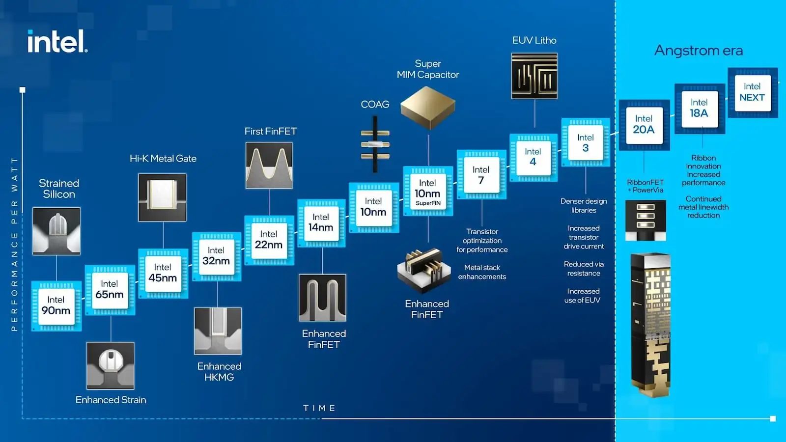
In the 2000s, processors were etched with a fineness of around 180 nm. Today, the most advanced technologies, such as those used by TSMC or Intel, reach 3 nm, or even less in future prototypes. This constant reduction is the result of a well-known law in computing: Moore’s Law, which predicts that the number of transistors on a chip doubles every two years.
Limited influence on performance
Contrary to popular belief, reduced engraving finesse does not always guarantee better performance. For example, a 7nm processor may perform less well than a 10nm one if its architecture (the way transistors are organized and used) is less optimized.
Processor performance depends on many other factors:
- CPU architecture: This is the “construction plan” that determines how the transistors interact.
- The number of cores: the more cores, the more tasks the processor can execute simultaneously.
- Frequency: Expressed in GHz, this indicates the speed at which each core can perform calculations.
This means that two processors with identical engraving finesse can offer very different performance levels.
What are the advantages of a smaller engraving fineness?
Engraving finesse is one of the most significant technological advances. But what are the real advantages of a smaller engraving finesse?
Better performance and computing power
Smaller etch sizes enable more transistors to be placed on the same silicon surface. The more transistors there are, the more operations a processor can perform simultaneously, which translates into considerable gains in computing power.
Processors etched in 7nm, for example, far surpass previous generations in terms of speed and efficiency.
Reducing energy consumption
Smaller transistors consume less energy to operate, which has two major effects:
- Extended autonomy for mobile devices. Smartphones and laptops benefit directly from this improvement, with longer-lasting batteries.
- A reduced ecological footprint. Less energy means less heat generated and therefore lower cooling requirements (important in data centers, intensive computing, etc.).
Component size reduction
Smaller engraving finesse enables more compact processors to be designed, while integrating more functions. This contributes to the miniaturization of electronic devices, making it possible to create ever lighter, thinner and more powerful gadgets.
For example, modern smartphones use chips engraved in ARM (Advanced RISC Machines) with impressive precision, enabling streamlined designs without compromising performance.
Etching finesse reaches its physical limits with silicon
For several decades, the semiconductor industry has pursued a relentless quest to reduce the etch fineness of electronic circuits. This has led to incredible progress in terms of performance, power consumption and component density on a chip. But today, as tech giants push back the frontiers of miniaturization, an inescapable reality is emerging: silicon, the basic material of semiconductors, is approaching its physical limits.
The miniaturization race: Where do we stand?
Today, the most advanced processors, manufactured by leaders such as TSMC, Samsung and Intel, achieve an etching fineness of 3 nm, and plans to go down to 2 nm are underway. However, each further reduction becomes a colossal technical challenge.
Silicon has physical limitations that complicate the continuous reduction of etch finesse:
- Quantum tunneling: At extremely small dimensions, electrons can “escape” through insulation barriers and cause current leakage.
- Exponential production costs: Manufacturing chips of lower finesse requires state-of-the-art equipment, such as extreme ultraviolet (EUV) lithography, which is astronomically expensive.


